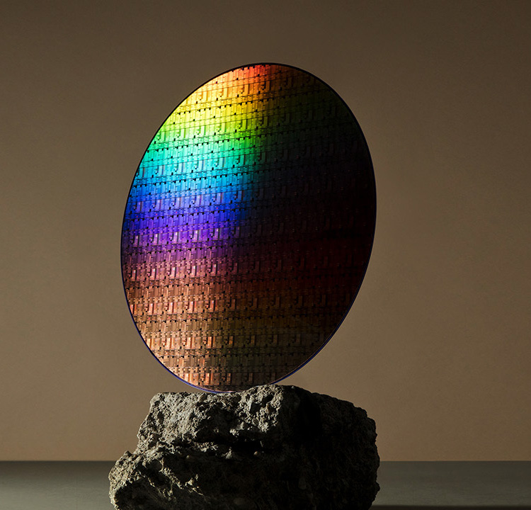
Samsung and IBM have designed a new vertical transistor architecture for semiconductors that promises reduced energy usage compared to scaled finFET semiconductors and potentially pave the way for semiconductors’ future while following the Moore’s Law principle.
Called as the Vertical Transport Field Effect Transistors or VTFET, the transistors are built perpendicular to the surface of the chip with a vertical, or up-and-down, current flow. This is different than the current structure where transistors are built to lie flat upon the surface of a semiconductor.
The researchers also claim that this process helps extending Moore’s Law as more transistors are packed in a fixed space and result in less wasted energy, which helps to reduce up to 85% energy compared to scaled finFET options.
Few advantages of this breakthrough is that smartphone batteries in the future can hold a week’s charge instead of days or cryptomining can consume less energy or expanded use of IoT devices.